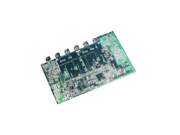
4 Layer PCB
4 Layer PCB
Specifications
1
4 Layer PCB
Inner copper thickness: 3oz
Finish outer copper thickness: 4oz
Solder mask: *2 Green
Base material: FR4, 2.4mm
Dimension: 500.0*360.12mm
Surface treatment: Lead-free HASL
3
4 Layer PCB
Base material: FR4, 1.6mm
Copper thickness: Inner (1oz), Outer (1oz)
Peelable solder mask: Peters SD2955
Min. track width/space: 0.15mm
Min. hole: 0.25mm
Surface treatment: Lead-free HASL
Structure | ||
Layer Count | 1, 2, 4, 6, 8, 10,12 | 1, 2, 4, 6, 8, 10, 12, 14, 16 |
HDI Technology | For Sample | Run Production |
Min. Board Thickness | 24mil | 24mil |
Max. Board Thickness | 126mil | 126mil |
Copper Foil | ||
Copper Foil Outer Layer | 1/2oz-10oz | 1/2oz-10oz |
Copper Foil Inner Layer | 1/2oz-3oz | 1/2oz-3o/z |
Drill | ||
Plating Hole Tolerance | /-3mil | /-3mil |
Non-plating Hole Tolerance | /-2mil | /-2mil |
Min. Drill Bit | 0.25mm | 0.25mm |
Dielectric Thickness | ||
Core Thickness (Min) | 3mil | 3mil |
Dielectric Thickness (prepreg) | 2mil | 2mil |
Finished Board Thickness Tolerance | /-10% FBT>=50mil /-12% 24mil=<50mil /-3milFBT<24mil | /-10% FBT>=50mil /-12% 24mil=<50mil /-3milFBT<24mil |
Solder Mask | ||
Solder Mask Dam (Min.) | 3mil | 3mil |
Solder Mask Opening (Min.) | 2.5mil | 2.5mil |
Solder Mask Plug Hole Size | 0.3mm-0.7mm | 0.25mm-0.7mm |
Registration Capability | ||
Layer to Layer | 3mil | 3mil |
Plating Capability | ||
Aspect Ratio (Mechanical) | 10 : 1 | 12 : 1 |
Aspect Ratio (Laser) | 0.8 : 1 | 0.8 : 1 |
Electrical / RF Capability | ||
Min. Line Width/Space (Inner ½oz) | 4mil / 4mil | 4mil / 4mil |
Min. Line Width/Space(Inner1oz) | 4mil / 4mil | 4mil / 4mil |
Min. Line Width/Space(Outer1/2oz) | 4mil / 4mil | 4mil / 4mil |
Line Tolerance | /-20% | /-20% |
Impedance | ||
Impedance Control | YES | YES |
Impedance Tolerance | /-10% | /-10% |
Outline | ||
Routing Tolerance | /-5mil | /-5mil |
Punching Tolerance | /-4mil | /-4mil |
V-cut Angle | 30degree, 45degree, 60degree | 30degree, 45degree, 60degree |
V-cut Tolerance | /-3degree | /-3degree |
V-cut Web Thickness Tolerance | /-3mil | /-3mil |
Surface Finished | ||
Organic Solderability Preservative | Yes | Yes |
Electroless Nickel / Immersion Gold | Yes | Yes |
Immersion Silver | Yes | Yes |
Lead Free HASL | Yes | Yes |
Immersion Tin | Yes | Yes |
E-Test | ||
Test Voltage | 25v-250v | 25v-250v |
Insolation Resistance | 2M ohms-100M ohms | 2M ohms-100M ohms |
Continuity | 5 ohms–1k ohms | 5 ohms –1k ohms |
Others | ||
Lead Time | Prototype: Single side: 2 days Double side: 3 days Multilayer: 6 days | Production: Single side: 5-7 days Double side: 7 days Multilayer: 9 days |
Honya International is a leading 4 layer PCB manufacturer, located in China. In addition to 4 layer PCB, we also provide FPC, aluminium base PCB, double side PCB, and related products. Due to high quality and reasonable prices, our printed circuit board or PCB is popular among the clients from Spain, UK, USA, Netherlands, Germany, Brazil, India, among others.
Thank you for visiting our website. We at Honya welcome you to contact us for more information!
Links:https://www.globefindpro.com/products/105414.html
-
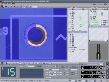 Optical Measurement Machine (CCD Camera)
-
 Tea Bag Packaging Machine B.DP
-
 Coordinate Measuring Machine (Bridge Type)
-
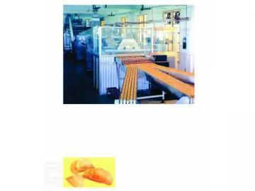 Compound Potato Slice Equipment
-
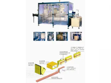 Self Adhesive Labeling Machine, B.ZX120 Horizontal Type
-
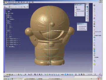 3D Laser Scanner
-
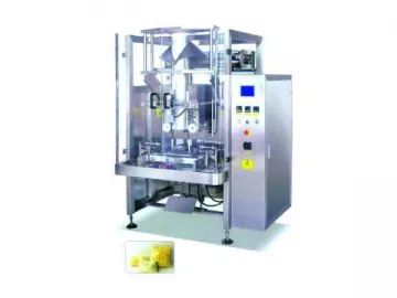 Large Vertical Form-Fill-Seal Machine
-
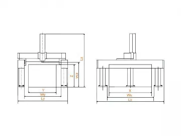 Coordinate Measuring Machine (Gantry Style)
-
 Packing Machine, B.ZD Intelligent Automatic Type
-
 Stand-Up Pouch Packaging Machine, S-180D Horizontal Automatic Type
-
 Yoghourt Soft Candy Production Line (Jelly Grains / Nuts Inside) S.NT-II
-
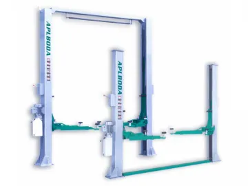 Hydraulic Car Lift (Two Post)
