ENIG PCB
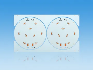
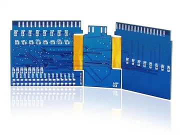
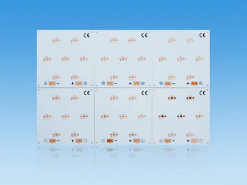
ENIG PCB stands for Electroless Nickel Immersion Gold PCB. Comparing to HASL and Immersion Silver, this PCB surface finish has been extensively applied to high-end PCB. The process of Electroless Nickel plating and immersion gold has been approved to be lead-free. Its ultra-flat surface provides stable welding spots and resistance to exterior environment and touching, etc. Quotation is offered via PCB Pro and Okey Custom System.
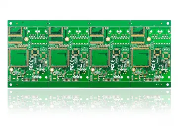
ENIG PCB has stable color and high bright surface. Ultra-flat pads are responsible for drastically reduced SMT difficulty. In particular, SMT for ultra-small substrates such as 0603 and 0402 can be a daunting job. Flatness of pads is the predominant factor in determining quality of printing and reflow soldering. Therefore, ENIG is frequently seen in SMT for high density and ultra-small PCB.
Thickness
Due to unsurpassed quality, ENIG PCB comes with relatively high cost. Moreover, we have the ability to meet your requirement on thickness of gold and nickel during PCB surface finishing.
Normal Gold (Au) Thickness: 2uin-5uin (0.05um-0.125um)
Normal Nickel (Ni) Thickness: 80uin-320uin (2um-8um)
Classification
1. Four Layer ENIG PCB
This wiring technology is endowed with impedance for signal reception and transmission. Interior impedance is 50 Ohm, and exterior impedance reaches 100 Ohm. PCB is 1.2mm thick, and vias come in 0.25mm diameter. Gold thickness is 2uin. Thanks to impedance, this ENIG PCB is perfect for signal transmission board and reception board.
2. Double Sided Half Hole ENIG PCB
Ingenious half hole design drills holes after electroplating for being burr-free and clean. Hole milling involves the utilization of new drilling tool for clean finish. Gold thickness reaches 3uin for best coating. FR-4 is adopted, and copper thickness is 35/35um. Half hole size is 0.4mm. This PCB is designed for signal conversion carrier.
3. Double Sided Speaker Board
Copper thickness swells to 175um by several times of electroplating and chemical gold thickness reaches over 5uin. Both sides have different gold thickness which respectively is 35um and 175um. This kind of PCB is designed for microphone and speaker.
4. Four Layer Card
0.3mm BGA and gold fingers are available by soldering and gold plating for PCB. When soldering, we use blue solder mask to protect gold fingers. This product is well-suited for memory bank and network card.
5. Gold Fingers Card
This card is distinguished by purple color and as many as 9 IC. Minimum PTH hole size is 0.25mm. Vias are covered by solder mask. This card is applicable for computer main board output.
Links:https://www.globefindpro.com/products/76096.html


