6 Layer PCB
6 Layer PCB
Specifications
2
6 Layer PCB
Inner copper thickness: 1oz
Outer copper thickness: 1oz
Solder mask: *2 Green
Base material: FR4, 1.6mm
Panel ups: 1*4
Surface treatment: Immersion gold
Min. hole: 0.25mm
5
6 Layer PCB with BGA
Base material: FR4, 1.6mm
Solder mask: Blue *2
Min. track width/space: 0.18mm
Min. hole: 0.2mm
Surface treatment: Immersion gold
7
6 Layer PCB
Base material: Fr4, 1.6mm
Solder mask: Green *2
Profile: Milling
Surface treatment: Immersion silver
No X-out allowed
| Structure | ||
| Layer Count | 1, 2, 4, 6, 8, 10,12 | 1, 2, 4, 6, 8, 10, 12, 14, 16 |
| HDI Technology | For Sample | Run Production |
| Board Thickness(Min.) | 24mil | 24mil |
| Board Thickness (Max.) | 126mil | 126mil |
| Copper Foil | ||
| Copper Foil Outer Layer | 1/2oz-10oz | 1/2oz-10oz |
| Copper Foil Inner Layer | 1/2oz-3oz | 1/2oz-3o/z |
| Drill | ||
| Plating Hole Tolerance | /-3mil | /-3mil |
| Non-plating Hole Tolerance | /-2mil | /-2mil |
| Min. Drill Bit | 0.25mm | 0.25mm |
| Dielectric Thickness | ||
| Core Thickness (Min.) | 3mil | 3mil |
| Dielectric Thickness (prepreg) | 2mil | 2mil |
| Finished Board Thickness Tolerance | /-10% FBT>=50mil/-12% 24mil=<50mil/-3milFBT<24mil | /-10% FBT>=50mil/-12% 24mil=<50mil/-3milFBT<24mil |
| Solder Mask | ||
| Solder Mask Dam (Min.) | 3mil | 3mil |
| Solder Mask Opening (Min.) | 2.5mil | 2.5mil |
| Solder Mask Plug Hole Size | 0.3mm-0.7mm | 0.25mm-0.7mm |
| Registration Capability | ||
| Layer to Layer | 3mil | 3mil |
| Plating Capability | ||
| Aspect Ratio (Mechanical) | 10 : 1 | 12 : 1 |
| Aspect Ratio (Laser) | 0.8 : 1 | 0.8 : 1 |
| Electrical / RF Capability | ||
| Min. Line Width/Space (Inner ½oz) | 4mil / 4mil | 4mil / 4mil |
| Min. Line Width/space(Inner1oz) | 4mil / 4mil | 4mil / 4mil |
| Min. Line Width/Space(Outer1/2oz) | 4mil / 4mil | 4mil / 4mil |
| Line Tolerance | /-20% | /-20% |
| Impedance | ||
| Impedance Control | YES | YES |
| Impedance Tolerance | /-10% | /-10% |
| Outline | ||
| Routing Tolerance | /-5mil | /-5mil |
| Punching Tolerance | /-4mil | /-4mil |
| V-cut Angle | 30degree, 45degree, 60degree | 30degree, 45degree, 60degree |
| V-cut Tolerance | /-3degree | /-3degree |
| V-cut Web Thickness Tolerance | /-3mil | /-3mil |
| Surface Finished | ||
| Organic Solderability Preservative | Yes | Yes |
| Electroless Nickel /Immersion Gold | Yes | Yes |
| Immersion Silver | Yes | Yes |
| Lead Free HASL | Yes | Yes |
| Immersion Tin | Yes | Yes |
| E-Test | ||
| Test Voltage | 25v-250v | 25v-250v |
| Insolation Resistance | 2M ohms-100M ohms | 2M ohms-100M ohms |
| Continuity | 5 ohms–1k ohms | 5 ohms –1k ohms |
| Others | ||
| Lead Time | Prototype: Single side: 2 daysDouble side: 3 daysMultilayer: 6 days | Production: Single side: 5-7 daysDouble side: 7 daysMultilayer: 9 days |
As an experienced 6 layer PCB manufacturer and supplier in China. Honya International can provide not only 6 layer printed circuit board, but also single side PCB, aluminium base PCB, flexible circuit, and more. Besides, located in Shenzhen, we enjoy convenient transportation by land, sea, and air. So we can deliver our printed circuit board quickly and cheaply.
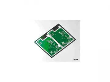
If you are interested in our circuit board, please continue browsing our corresponding webpage, or contact us for more product information. We at Honya are looking forward to hearing you.
Links:https://globefindpro.com/products/105427.html
-
 Coordinate Measuring Machine (L Style High Bridge Type)
-
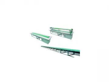 Self Adhesive Labeling Machine, B.TB-L Vertical Type
-
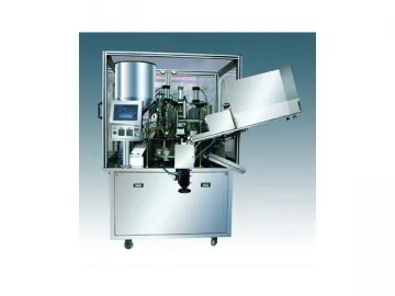 Packaging Machine, S-130 Horizontal Automatic Type
-
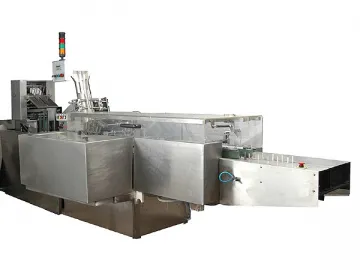 Box Sealing Machine B.FX
-
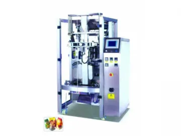 Vertical 4 Edge Sealing Form-Fill-Seal Machine
-
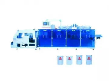 Stand-Up Pouch Packing Machine, S-180S Horizontal Automatic Type
-
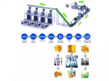 Automatic Solution Program
-
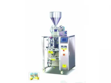 Vertical Liquid Form-Fill-Seal Machine
-
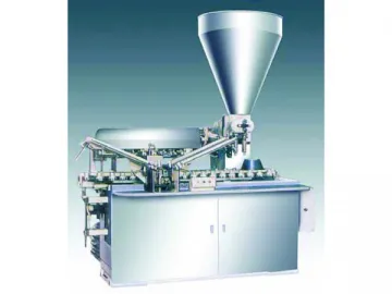 Packing Machine, B.ZB Multifunction Horizontal Type
-
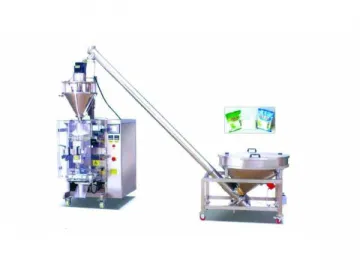 Vertical Powder Form-Fill-Seal Machine
-
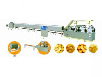 Automatic Biscuit Processing Line
-
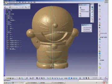 3D Laser Scanner

